Last updated on February 26, 2026, by Lucy
Many engineers feel stuck between slow PCB suppliers and urgent prototype deadlines. I have faced that pressure too. When speed matters, traditional fabrication often slows innovation.
A 3D printed PCB uses additive manufacturing to deposit conductive materials layer by layer instead of etching copper from FR4 sheets. It enables rapid prototyping, complex geometries, and low-volume production without tooling, but it has limits in conductivity, durability, and large-scale cost efficiency.

If you are new to additive manufacturing in general, I always suggest starting with a clear technical foundation. Understanding the basics of what 3D printing is helps clarify why printed electronics behave differently from traditionally fabricated boards.
I have worked with engineers who needed functional boards in days, not weeks. I have also seen projects fail because the wrong technology was chosen. So in this guide, I will break down where 3D printed PCBs truly fit in industrial and OEM environments, and where they do not.
What Is Additive PCB Manufacturing and Where Are Its Technical Limits?
Many teams hear the term “3D printed PCB” and assume it replaces traditional boards completely. That assumption creates unrealistic expectations and poor design decisions.
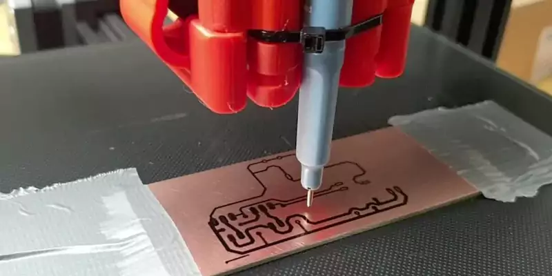
Additive PCB manufacturing builds conductive traces by depositing silver or copper-based inks layer by layer, unlike traditional subtractive PCB fabrication that etches copper from FR4 laminates. It supports rapid iteration and 3D integration but has conductivity, layer count, and thermal limitations compared to standard copper boards.
Additive vs. Subtractive Manufacturing
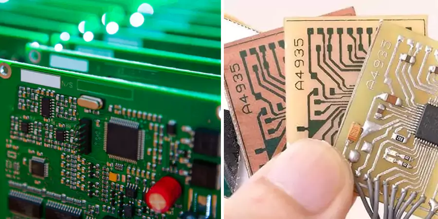
Traditional PCB fabrication uses FR4 sheets laminated with copper. The process removes copper through chemical etching. This method delivers high conductivity and multi-layer capability. It is stable for automotive and industrial mass production.
Additive PCB printing works differently. It deposits conductive ink directly onto polymer or high-temperature substrates. Some systems use silver nanoparticle ink. Others use copper-based materials. The board is built layer by layer.
In broader manufacturing strategy discussions, I often compare this shift to the decision between CNC and additive processes. If you want a deeper comparison framework, you can review how we analyze CNC machining vs 3D printing for mechanical parts. The same trade-off logic applies to electronics: speed and flexibility versus scalability and material performance.
Here is a simple comparison:
| Parameter | Traditional FR4 PCB | 3D Printed PCB |
|---|---|---|
| Conductor | Solid copper | Conductive ink |
| Tooling | Required | Not required |
| Typical Lead Time | 2–4 weeks | 2–5 days |
| Layer Count | 2–16+ layers | Usually 1–4 |
| Conductivity1 | Very high | Lower than copper |
Technical Boundaries
Conductivity is the first limitation. Copper has very low resistivity. Conductive inks have higher resistance. That means current carrying capacity is limited.
Minimum trace width also depends on printer resolution. Many systems support 100–200 microns. That is fine for signal circuits. It is not ideal for high-power modules.
Thermal performance2 is another concern. Polymer substrates do not dissipate heat like metal-backed PCBs. So high-current automotive power modules are not suitable.
I always tell clients this: 3D printed PCBs are strong in flexibility and speed. They are weak in high-volume, high-current, high-temperature applications.
How Should Engineers Design 3D Printed PCBs for Automotive and Industrial Use?
Some engineers reuse traditional PCB rules without adjustment. That approach often causes rework and signal problems.
Design for Additive Electronics requires adjusting trace width, current density, via design, and thermal management strategies. Engineers must account for higher resistance, limited layer stacking, vibration exposure, and regulatory compliance in automotive and medical environments.
Design for Additive Electronics (DfAE)
Trace routing must account for higher resistance. I usually increase trace width3 by 20–40% compared to copper designs when current exceeds 1A.
Via formation is limited by material curing and deposition accuracy. Blind vias are often easier than complex buried structures.
Embedded components are possible. However, they require early planning. Mechanical and electrical integration must be designed together.
In practice, this is where strong additive manufacturing capability matters. A supplier with mature 3D printing capabilities can control layer adhesion, dimensional accuracy, and material curing consistency. That directly affects trace reliability and long-term performance.
Environmental and Reliability Constraints
In automotive modules, vibration matters. I once supported a small automotive sensor housing project. The board was printed and integrated into a CNC-machined aluminum enclosure.
Here were the test parameters:
| Test Item | Parameter | Result |
|---|---|---|
| Vibration | 10–500 Hz sweep | Passed |
| Temperature Cycle | -20°C to 85°C, 100 cycles | No trace cracking |
| Continuous Current | 1.5A | Stable |
| Resistance Increase | <8% after testing | Within tolerance |
The aluminum housing helped manage heat. The enclosure also protected the board from mechanical stress.
For medical devices, sterilization chemicals may degrade some polymers. So material selection is critical.
Compliance also matters. RoHS and CE marking requirements must be considered early. IPC guidance still applies, even if the process differs.
Is 3D Printed PCB More Cost-Effective or Just Faster?
Many procurement managers assume additive means cheaper. That assumption is not always true.
3D printed PCBs reduce tooling and setup costs and dramatically shorten lead time, but per-unit cost is often higher than traditional fabrication in medium or high volumes. They are most cost-effective for prototypes and low-volume runs.
Cost Structure Breakdown
There is no photomask. There is no etching bath. That reduces upfront cost.
Lead time can drop from three weeks to three days. That is a major advantage in R&D.
However, material cost per board is higher. Conductive inks are expensive.
Here is a simplified break-even example I use:
| Volume | Traditional PCB Cost/Unit | 3D Printed PCB Cost/Unit |
|---|---|---|
| 10 pcs | $45 | $38 |
| 100 pcs | $18 | $28 |
| 1000 pcs | $6 | $22 |
So at low volume, additive wins. At higher volume, traditional wins.
There are also hidden costs. Reliability testing takes time. Certification costs money. Assembly compatibility must be checked.
I see 3D printed PCBs as a rapid prototyping tool. They are similar to rapid metal prototypes. They are not universal replacements.
How Can 3D Printed PCBs Integrate with CNC Machined Components?
Many projects fail because electronics and mechanical design are treated separately. I have learned that integration creates the real advantage.
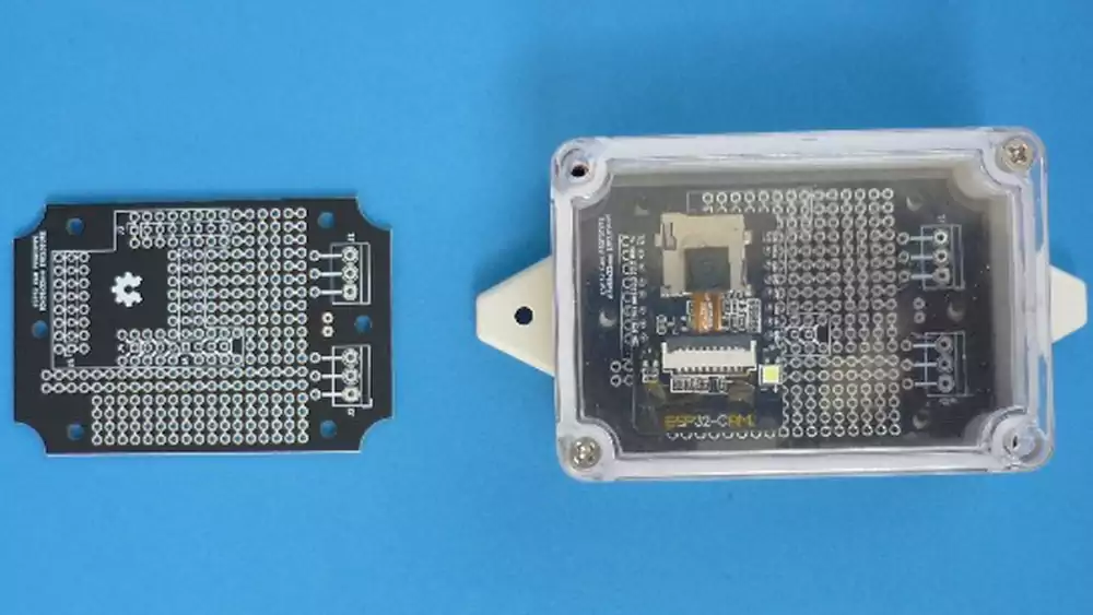
3D printed PCBs integrate effectively with CNC machined aluminum housings, custom heat sinks, and lightweight structural assemblies, enabling compact sensor modules, industrial monitoring devices, and rapid mechanical-electrical prototypes.
Mechanical-Electrical Integration
CNC machining allows precise aluminum enclosures. These housings improve thermal management. They also protect sensitive traces.
I once worked on an industrial monitoring unit for a robotics client. The printed PCB was mounted inside a 6061-T6 aluminum housing4.
Key specs:
| Parameter | Value |
|---|---|
| Housing Material | 6061-T6 Aluminum |
| Machining Tolerance | ±0.02 mm |
| Surface Finish | Anodized |
| PCB Current | 1.2A |
| Operating Temp | 0–70°C |
The machined housing reduced surface temperature by 12°C compared to a plastic enclosure. That improved long-term stability.
Why Integration Matters
When I combine 3D printed electronics with precision CNC machining, I can control mechanical fit, heat transfer, and structural rigidity.
That combination supports automotive sensor modules, motorcycle control units, medical handheld devices, and industrial automation systems.
3D printed PCBs are not for everyone. They are like rapid prototyping for metal parts. When complexity is high and speed is critical, nothing else compares.
Conclusion
3D printed PCBs are powerful for rapid, low-volume, and integrated applications, but they require careful engineering judgment and are not replacements for traditional mass-production boards.
-
Explore this link to understand why conductivity differences impact PCB performance and application suitability. ↩
-
Learn about thermal management challenges in PCBs to choose the right technology for high-power applications. ↩
-
Explore this resource to understand how adjusting trace width impacts current capacity and reliability in PCB design. ↩
-
Explore this link to understand why 6061-T6 aluminum housing is preferred for thermal management and protection in electronics. ↩
